Digital image processing is the core technology behind modern photography. In the digital era, cameras have evolved from simple light-capturing tools to intelligent machines capable of turning light into highly detailed images. This transformation is achieved through a sequence of electronic and computational stages inside the camera — starting from the moment light hits the sensor to when the final image is stored on a memory card.
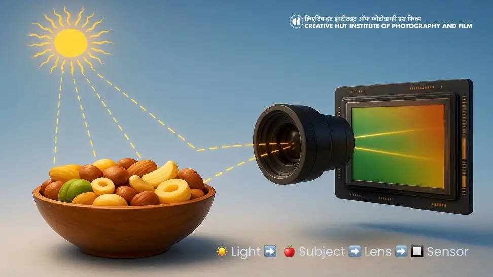
☀️ Light ➡️ 🍎 Subject ➡️ Lens ➡️ 🔲 Sensor
THE DIGITAL IMAGING WORKFLOW
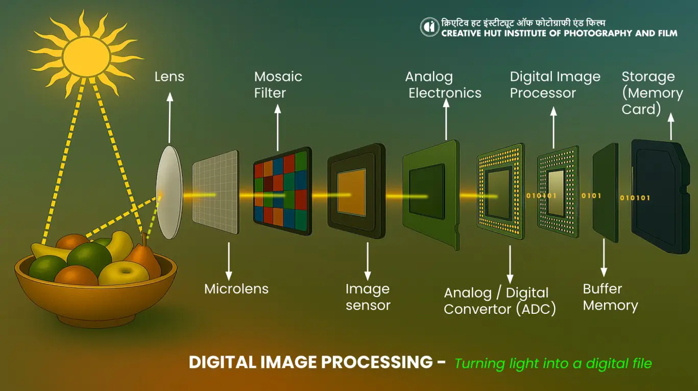
☀️ Sun → 🍎 Subject → 📷 Lens → 🔲 Microlens Array → 🎨 Mosaic Bayer Color Filter → 🔲 Image Sensor → ⚡ Analog Electronics → 🔄 Analog/Digital Converter (ADC) → 🔲 Digital Image Processor → 📂 Buffer Memory → 💾 Storage (Memory Card)
Photon → Electron → Voltage → Binary Digital Data
The process begins when light reflects off a subject and enters the camera lens. From there, the journey of the image follows a specific path:
Sun – Primary light source that illuminates the subject, providing the photons necessary for image capture.
Subject – The object or scene being photographed; it reflects or emits light toward the camera.
Lens – Focuses incoming light onto the camera’s sensor system, controlling sharpness and image framing.
Microlens Array – A grid of tiny lenses placed over each pixel to direct light more efficiently onto the sensor’s photodiodes.
Mosaic Bayer Color Filter – A color filter pattern (typically red, green, and blue) laid over the sensor to capture color information for each pixel.
Image Sensor – Captures the filtered light and converts it into an electrical signal (photons → electrons).
Analog Electronics – Processes and stabilizes the weak analog signal from the sensor to prepare it for digitization.
Analog/Digital Converter (ADC) – Converts the prepared analog signal into digital binary data (0s and 1s).
Digital Image Processor – Applies computational enhancements such as color correction, sharpening, tone mapping, and noise reduction.
Buffer Memory – Temporarily stores the processed image data while the camera writes it to permanent storage.
Memory Card – Permanently stores the final image file in formats like JPEG or RAW for later retrieval.
Image Sensors and Pixel Structure
A digital image sensor is a solid-state silicon chip made up of a grid of photosensitive elements called pixels (or photosites). These pixels are semiconductor-based and are responsible for absorbing incoming light (photons) and converting it into an electric charge (electrons). The more light a pixel receives, the more charge it generates, forming the raw image data.
Each pixel typically includes:
A microlens to focus light onto the sensor.
A color filter (in color sensors).
A photodiode to convert light into electricity.
A potential well to hold the charge.
An amplifier to boost the signal.
The sensor chip is protected by a cover glass and packaging that shields it from physical and environmental damage, dissipates heat, and houses wire bonds that transfer data to the camera’s main board.
Sensor Construction
Digital image sensors are built with multiple precision-engineered layers that work together to ensure accurate and efficient light capture.
Cover Glass: This is a transparent protective layer placed over the sensor. It safeguards the delicate sensor chip and its internal wiring from dust, scratches, and physical damage without interfering with light transmission.
Packaging: The sensor packaging provides structural protection and plays a key role in heat dissipation. It also includes the electrical pathways needed to transfer image data from the chip to the rest of the camera circuitry.
Sensor Chip: At the core of the sensor is a thin layer of silicon. When photons strike the silicon surface, the chip generates electrons — a process that converts light into an analog electrical signal. This is the foundation of digital imaging.
Wire Bonds and Contact Pads: These fine wire connections transmit the electrical signals generated by each pixel to the contact pads located on the rear of the sensor. From there, the data continues to the camera’s processing system.
Sensor Classifications
Sensors can be categorized based on different technical parameters:
Structure Type: CCD (Charge-Coupled Device) or CMOS (Complementary Metal-Oxide Semiconductor).
Chroma Type: Color or monochrome sensors.
Shutter Type: Global shutter or rolling shutter.
Additional Parameters: Resolution, pixel size, frame rate, and sensor format.
Pixels and Image Quality
Pixels are arranged in a grid pattern across the surface of the sensor. Each pixel is like a tiny light-sensitive square. The number of pixels (rows × columns) determines the resolution of the image.
Pixel Size: Measured in microns (µm). Larger pixels can absorb more light and produce better image quality, especially in low-light conditions. For example, smartphone sensors may use 1.1 µm pixels, while full-frame cameras may use pixels as large as 8.4 µm.
Pixel Pitch: The center-to-center distance between adjacent pixels. This measurement helps determine how tightly packed the pixels are. Note that pixel pitch doesn’t always represent the exact size of a pixel due to gaps between them.
Microlens and Light Efficiency
Modern sensors feature microlenses positioned above each pixel. These lenses direct and concentrate incoming light onto the photosensitive area of the pixel. This design improves the sensor’s ability to collect light efficiently, reduces light loss, and enhances overall image quality — especially in small-pixel sensors like those found in mobile phones.
Bayer CFA Sensor
A Bayer Color Filter Array (CFA) is a grid of red, green, and blue color filters placed over the image sensor to capture color information. Each pixel on the sensor is covered with a single color filter—either red, green, or blue—making it sensitive to only one wavelength of light. The most common CFA is the Bayer pattern, invented by Bryce Bayer.
The Bayer pattern arranges the filters as:
50% Green
25% Red
25% Blue
The Bayer filter layout takes advantage of the human eye’s increased sensitivity to green by using a 2×2 repeating grid that contains twice as many green filters as red or blue. This pattern alternates rows of red and green filters with green and blue, ensuring that green-sensitive pixels are more frequent to enhance image luminance and clarity. The Bayer filter is positioned between the microlens and the photodiode in each pixel, allowing only one specific color wavelength to pass through to the sensor.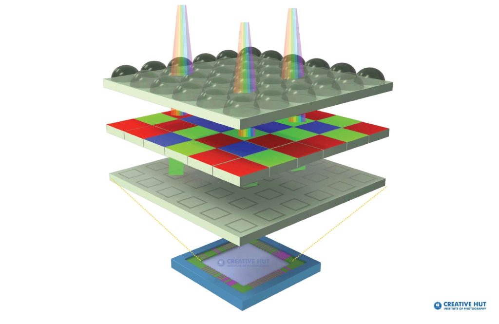 Operation of the Bayer filter
Since each pixel captures only one color component, a process called demosaicing is used to interpolate and reconstruct a full-color image by combining data from neighboring pixels. This technique allows the sensor to deliver realistic color images despite each pixel capturing only a single color value.
Each pixel on a Bayer sensor has only one color filter — either red, green, or blue — placed over it. That means a single pixel can detect only one color, not all three. The camera uses data from neighboring pixels to reconstruct the full-color image through a process called demosaicing.
Most modern digital cameras use the Bayer CFA because of its balance between color accuracy and efficiency. However, alternative color filter arrays with different patterns also exist. In contrast, monochrome (mono) sensors do not have a color filter array, meaning each pixel is sensitive to the entire visible light spectrum, resulting in higher detail and sensitivity.
Did You Know?
The Bayer Color Filter Array was invented by scientist Bryce E. Bayer in 1976 while working at Eastman Kodak. His design allowed image sensors to capture color using a grid of red, green, and blue filters. Due to his contribution, this filter arrangement is known as the Bayer Pattern. In a sensor’s pixel structure, the Bayer filter is positioned between the microlens and the photodiode, where it filters incoming light so that each pixel records only one color channel.
Photodiode
At the heart of each pixel in a digital image sensor lies a photodiode — a semiconductor device responsible for converting light into an electrical signal. Technically, a photodiode is made up of a p-n junction, which allows it to generate electrical current when exposed to light. When photons (light particles) strike the photodiode, they are absorbed and release electrons. The number of electrons produced corresponds to the intensity of the light received. This conversion process forms the foundation of the analog signal used to construct digital images.
Potential Well
After photons are converted into electrons by the photodiode, the resulting electrical charges need to be stored for further processing. This storage takes place in a small, bucket-like region inside each pixel, known as the Potential Well.
The potential well acts like a container that collects and holds the free-flowing electrons generated from the incoming light. The number of electrons it can hold before becoming full is called its Full Well Capacity.
Larger pixels have deeper potential wells, which means:
They can hold more charge,
They offer higher sensitivity to light,
They produce a better signal-to-noise ratio (SNR), and
They support a wider dynamic range, capturing both shadows and highlights with more detail.
In simple terms, the potential well determines how much light information a pixel can store before reaching its limit — and this directly affects image quality.
Think of the potential well as a water bucket — more light (photons) means more water (electrons). If the bucket is too small, it overflows — which is why bigger wells in larger pixels help store more information without losing detail.
Amplifier
In the process of digital image capture, the amplifier plays a key role in strengthening the weak electrical signals generated by the photodiodes. In CMOS sensors, each pixel has its own amplifier, typically placed at the corners of the pixel. This design allows the sensor to read and process pixel signals individually and in parallel, making CMOS sensors faster and more efficient in many modern cameras.
In contrast, CCD sensors use a different system. There is usually only one amplifier for the entire sensor array. Here, the charge from each pixel is transferred sequentially, starting from the first row. The amplifier reads the charge from the first pixel, amplifies it, and passes it along. Once that pixel is read, it is cleared, and the process repeats with the next pixel in line. This continues until the entire row is processed.
After a full row is read and emptied, the sensor shifts the remaining charges downward, row by row, so that the next row can be read by the amplifier. This movement resembles a cascading flow of data from the top to the bottom of the sensor.
Before sending the signal for further processing, the amplifier also tags each charge — assigning it a positional identifier. This ensures that when the digital image is reconstructed, each pixel’s data is reassembled in the correct order, preserving the structure and clarity of the original scene.
Quantum Efficiency (QE)
The first step in capturing a digital image is the conversion of photons into electrons. This process happens at the pixel level inside the image sensor. The effectiveness of this conversion is measured by a value known as Quantum Efficiency (QE).
Quantum Efficiency is defined as the ratio of the number of electrons generated to the number of photons received by a pixel during the exposure time. It is expressed as a percentage.
A higher QE indicates that the sensor is more sensitive to light and is capable of capturing brighter, more detailed images, especially in low-light conditions.
Quantum efficiency varies across different sensor technologies and wavelengths of light. In general, modern CMOS sensors have significantly improved QE compared to older designs, making them more efficient and better suited for high-resolution, low-light photography.
Types of Color Filter Array (CFA) Sensors
In most digital cameras, Color Filter Arrays (CFAs) are used to capture color information. These arrays sit on top of the sensor and allow it to distinguish between different colors of light. There are two primary types of sensors that use CFAs: the Bayer CFA sensor and the Foveon sensor.
Bayer CFA Sensor – The Conventional Choice
The Bayer CFA (Color Filter Array) sensor is the most commonly used in digital imaging. It uses a grid of color filters arranged in a 2×2 repeating pattern—typically consisting of two green, one red, and one blue photosite. This pattern reflects the human eye’s greater sensitivity to green light.
Each pixel in a Bayer sensor measures only one color component—red, green, or blue. To produce a full-color image, the missing color information for each pixel is estimated using a process called demosaicing. While effective, this interpolation step can sometimes lead to slight color inaccuracies or artifacts.
Bayer CFA sensors are widely used in consumer and professional cameras, including Nikon, Canon, and Sony systems. There are variations to the traditional Bayer pattern. For example:
Fujifilm’s X-Trans sensors use a more complex 6×6 grid to reduce moiré without using an optical low-pass filter.
Some sensors use CYGM (Cyan, Yellow, Green, Magenta) or RGBE (Red, Green, Blue, Emerald) filters for broader color capture.
Foveon Sensor – Capturing Full Color at Every Pixel
The Foveon sensor, developed and used by Sigma, takes a fundamentally different approach. Instead of using separate color filters for each pixel, the Foveon sensor uses three stacked photodiode layers made from silicon. Each layer captures a different color:
Top layer: Blue light
Middle layer: Green light
Bottom layer: Red light
This layered structure works because silicon absorbs different wavelengths of light at different depths. As a result, each pixel location captures full RGB color information, eliminating the need for demosaicing or interpolation.
This technology allows the Foveon sensor to produce highly detailed and color-accurate images, especially at low ISO values. However, Foveon sensors tend to have limitations in low-light performance, processing speed, and ISO range compared to Bayer sensors.
Constant Sensor Innovation
Both Bayer and Foveon sensors have seen improvements over time. Manufacturers continue to enhance sensor technologies by increasing:
Sensor size
Resolution
Low-light sensitivity
Processing speed
We also see a trend toward adding more color filters (like cyan or emerald) and creating hybrid sensors that combine the best features of both designs.
Both CCD (Charge-Coupled Device) and CMOS (Complementary Metal-Oxide-Semiconductor) sensors can be built using Bayer or other CFA patterns. They share the function of converting light into electrical charges, but the way they handle those charges differs:
CCD sensors move the electrical charge across the chip and read it at one corner using a single amplifier. This allows for high image uniformity but consumes more power and works slower.
CMOS sensors use individual amplifiers for each pixel, allowing for faster processing, lower power consumption, and better integration with on-chip processing — but sometimes at the cost of slightly more noise.
In both cases, the color filter array sits above the sensor, separating incoming light into red, green, and blue components — mimicking how the human eye perceives color.
Both Bayer CFA sensors and Foveon sensors are designed to capture color in digital images, but they use different methods.
The Bayer sensor captures only one color per pixel (red, green, or blue), relying on a repetitive 2×2 filter pattern across the sensor. This design requires a post-processing step called demosaicing to reconstruct the full-color image. Despite this, Bayer sensors are widely used due to their efficiency, low power usage, and good low-light performance. They are the standard in most digital cameras, including those by Nikon, Canon, Sony, and others.
In contrast, the Foveon sensor captures full RGB color at every pixel location by stacking three light-sensitive layers within a single pixel. This eliminates the need for demosaicing and offers superior color accuracy and fine detail, especially in well-lit conditions. However, Foveon sensors are typically limited to Sigma cameras and may not perform as well in low-light or high ISO settings due to slower signal readout and noise performance.
Both sensor types can be implemented using CCD or CMOS technology, which determines how the electrical signals are processed. CMOS sensors dominate today’s market due to their speed, energy efficiency, and integration flexibility, while CCDs offer more uniform image quality at the cost of slower readout and higher power consumption.
CCD | Charge-Coupled Devices
While the fundamental mechanism of image formation in Charge-Coupled Devices (CCDs) remains consistent—converting incident light into electrical charge and transferring that charge for output—variations in sensor architecture result in distinct operational behaviors. These differences form the basis for two primary classifications of CCD sensors: Interline Transfer (IT) and Full-Frame (FF) CCDs.
Interline Transfer (IT) CCD
The Interline Transfer CCD incorporates a configuration in which each vertical column of image pixels is paired with a dedicated vertical shift register, commonly referred to as an interline mask. These shift registers are optically shielded to prevent further exposure to light once the charge is transferred.
In this architecture, photons incident on the photosensitive surface are first converted into electrons within the photodiode. After the exposure is complete, each pixel’s charge is shifted horizontally into the adjacent interline register. These charges are then moved vertically down through the shift register columns into a horizontal shift register located at the base of the sensor. The horizontal register sequentially delivers each charge packet to the readout unit, where it is processed by a capacitor and amplifier circuit to produce an analog voltage. This voltage is subsequently digitized by an Analog-to-Digital Converter (ADC), enabling the image processor to reconstruct the final digital image.
The Interline Transfer architecture allows for rapid image acquisition and efficient charge handling, making it particularly suitable for applications such as digital video, machine vision, and real-time industrial imaging. However, due to the presence of shift registers occupying physical space on the sensor surface, there is a trade-off in terms of fill factor and light sensitivity, as not all pixel area is dedicated to light capture.
Full-Frame (FF) CCD
The Full-Frame CCD represents a traditional architecture in which the entire sensor surface is photosensitive, with no adjacent vertical transfer registers. Instead, charge transfer occurs directly within the pixel matrix itself.
Each pixel contains a vertical shift capability, allowing the accumulated charge to be transferred line by line to the horizontal readout register. Once positioned, each pixel’s charge is sequentially read, forming what is commonly referred to as a progressive scan.
It is important to note that the term “Full Frame CCD” refers to the complete utilization of the sensor’s surface area for light collection, and should not be confused with full-frame format (i.e., 36×24 mm sensor size in photography). Because all pixels remain light-sensitive during the readout process, mechanical or electronic shutters are generally required to prevent image smear or distortion.
Frame Transfer (FT) CCD – A Variant of the Full-Frame Model
A notable variation of the Full-Frame CCD is the Frame Transfer CCD. In this model, the sensor is divided into two equal-sized regions: a light-sensitive image area, and an adjacent light-shielded frame storage area.
Once exposure concludes, the entire charge pattern is quickly transferred from the imaging area to the storage region. This transfer happens fast enough to prevent further exposure during readout. The image is then read from the storage area in a manner similar to the Full-Frame model. This architecture allows for quicker capture intervals and is particularly advantageous in digital cinematography, scientific imaging, and high-frame-rate video recording.
Structural Arrangement and Signal Flow
In all three CCD variants, pixels are arranged in a matrix of horizontal and vertical rows. However, the spacing and function of adjacent elements differ depending on the sensor type. In Interline Transfer CCDs, vertical shift registers are physically positioned between columns of image pixels, requiring careful spacing and optical shielding. In contrast, Full-Frame and Frame Transfer CCDs allow a more compact arrangement of pixels, optimizing light collection but necessitating more complex readout timing.
The classification of CCDs into Interline Transfer and Full-Frame types represents not only architectural differences but also trade-offs between speed, sensitivity, and design complexity. Interline Transfer CCDs are suited for applications where readout speed and video capture are critical, while Full-Frame and Frame Transfer CCDs offer higher image quality and greater light sensitivity, often at the cost of slower readout and the requirement for external shutters.
A comprehensive understanding of these sensor designs is essential when evaluating imaging systems for scientific, industrial, or artistic purposes.
CMOS | Complementary Metal-Oxide Semiconductor
The Complementary Metal-Oxide Semiconductor (CMOS) image sensor has emerged as a pivotal advancement in digital imaging technology. Originally developed as a semiconductor process, CMOS was adapted for imaging applications in 1995 by Dr. Eric R. Fossum at the NASA Jet Propulsion Laboratory. His invention of the active pixel sensor (APS) laid the groundwork for the widespread integration of CMOS sensors in both consumer and professional imaging devices. Distinguished by their low power consumption, high processing speed, and cost efficiency, CMOS sensors have since become the predominant architecture in digital cameras and imaging systems.
Structural Architecture
CMOS sensors consist of a two-dimensional array of pixels arranged in rows and columns, analogous to the structure of CCD (Charge-Coupled Device) sensors. However, unlike CCDs, CMOS sensors do not employ centralized shift registers for charge readout. Instead, each pixel operates independently, integrating key processing elements locally.
A typical CMOS pixel unit comprises:
A photodiode, which converts incident photons into electrons,
Three transistors:
A reset transistor to initialize the pixel,
A source-follower amplifier for in-pixel signal amplification and charge-to-voltage conversion,
A row select transistor to enable readout of the pixel’s voltage.
This decentralised design allows for direct electrical readout at the pixel level, enabling parallel processing, faster frame rates, and reduced power consumption.
Operational Principles
Upon exposure to light, photons are absorbed by the photodiode in each pixel, generating a quantity of electrons proportional to the light intensity. These electrons are accumulated in a potential well located beneath the photodiode. The stored charge is then converted into a voltage and amplified on-site within the pixel circuitry.
The readout process occurs row by row:
A pixel select switch activates a horizontal row,
A column select switch enables access to each column’s pixel output,
The voltage signals are transmitted to a readout amplifier and subsequently digitized.
Modern CMOS designs may feature a shared or per-column analog-to-digital converter (ADC); more advanced implementations are exploring per-pixel ADC integration, further enhancing speed and reducing analog signal degradation.
Conceptual Analogy for CMOS Operation
To visualize the functioning of a CMOS sensor, one may consider the analogy of collecting colored raindrops into buckets:
Photons are equivalent to raindrops,
The microlens above each pixel focuses these “raindrops” into the collection bucket,
A Bayer filter, comparable to a colored cloth, filters the raindrops by color (red, green, or blue),
The bucket represents the potential well,
The amplifier functions like a pump, transferring the water (charge) for processing.
This analogy underscores the spatial and functional modularity of CMOS architecture, wherein each pixel performs both light capture and signal processing.
Advantages over CCD Technology
One of the defining features of CMOS image sensors is their exceptional energy efficiency, reportedly consuming up to 100 times less power than comparable CCD sensors. In addition to lower power requirements, CMOS sensors offer:
High-speed parallel readout,
Lower production cost due to standard semiconductor fabrication,
Smaller system footprint due to on-chip integration of image processing functions.
These characteristics make CMOS sensors particularly suitable for applications demanding real-time processing, high frame rates, and compact form factors, including mobile devices, machine vision, automotive systems, and medical imaging.
Photodiode and Fill Factor Considerations
In CMOS sensors, only the photodiode is optically active; the remaining pixel area is occupied by transistors and supporting circuitry. This distribution reduces the fill factor, defined as the ratio of light-sensitive area to total pixel area. To mitigate this limitation, manufacturers implement microlens arrays that concentrate incoming light onto the photodiode, effectively enhancing photon capture efficiency without enlarging pixel size.
Additionally, the well depth beneath each photodiode dictates the sensor’s full-well capacity, which directly influences its dynamic range and signal-to-noise ratio (SNR).
Future Developments
The evolution of CMOS sensors continues to advance toward greater integration, miniaturization, and functional density. Emerging designs are expected to include per-pixel analog-to-digital converters, improved noise reduction algorithms, and stacked sensor architectures, which further decouple the photodiode layer from the logic and processing layers. These innovations promise to enhance overall image quality, particularly in low-light conditions, and support broader adoption in computational photography and artificial intelligence-assisted imaging.
CMOS image sensors represent a convergence of photonics and microelectronics, delivering high performance, scalability, and cost-effectiveness. With continued advancements in semiconductor technology, CMOS sensors are expected to remain the cornerstone of digital imaging systems across diverse sectors—from professional photography and cinematic production to biomedical diagnostics and autonomous navigation.
STRUCTURE CMOS SENSOR
Modern CMOS (Complementary Metal-Oxide-Semiconductor) sensors have become essential in digital imaging, owing to their ability to convert light into electronic signals with high efficiency and compact form factor. As image resolution and low-light performance demands increase, innovations in sensor architecture have become crucial. One of the most significant architectural evolutions in CMOS sensors is the development of illumination directionality—specifically, the distinction between Frontside Illumination (FSI) and Backside Illumination (BSI).
These two designs differ in how photons reach the photodiodes embedded within each pixel, and each has distinct implications for sensor performance, quantum efficiency, and miniaturization. Understanding this distinction is critical for analyzing the behavior and capabilities of digital cameras across professional, scientific, and consumer imaging systems.
Frontside Illumination (FSI): Traditional Photodiode Orientation
Frontside illumination is the conventional layout found in early CMOS sensor designs. In this configuration, light enters the sensor from the same side as the metal wiring and transistor layers. As a result, photons must pass through several non-light-sensitive layers before reaching the photodiode. This structure not only reduces the effective amount of light reaching the sensor but can also introduce optical distortions and interference.
A notable drawback of FSI sensors is crosstalk, a phenomenon in which incoming photons are scattered by wiring layers and reach adjacent pixels, thus reducing image sharpness and color fidelity. To minimize such interference, manufacturers have developed guiding structures such as light tunnels—reflective channels that help direct photons to the appropriate photodiode. While helpful, this solution is limited, particularly in sensors with smaller pixel sizes.
Backside Illumination (BSI): Enhanced Sensitivity Through Reverse Architecture
Backside illumination emerged as a solution to the optical inefficiencies of the FSI layout. In BSI sensors, the photodiode is reoriented so that light enters from the opposite side—bypassing the obstructive layers of wiring and transistor gates. This reversal significantly improves quantum efficiency by allowing more photons to directly reach the photosensitive areas without interference.
The architecture enhances fill factor, enabling a larger portion of each pixel to respond to light. This directly translates into improved low-light performance, higher dynamic range, and greater image clarity. BSI technology is especially advantageous in compact sensors found in smartphones, action cameras, and scientific imaging tools, where maximizing light sensitivity in a constrained space is critical.
An industry example includes Sony’s Exmor R sensor, which leverages backside illumination to produce high-quality images even under challenging lighting conditions.
The evolution from frontside to backside illumination represents a pivotal advancement in CMOS sensor design. While FSI continues to be utilized in cost-sensitive applications, BSI sensors have redefined expectations for high-performance digital imaging. Their ability to enhance photon capture and minimize interference positions them at the forefront of current and future sensor technologies, driving innovation in fields ranging from consumer electronics to aerospace imaging systems.
CCD and CMOS
The two primary technologies used in modern digital image sensors are the Charge-Coupled Device (CCD) and the Complementary Metal-Oxide-Semiconductor (CMOS). While both serve the same fundamental purpose—converting light into electrical signals—they differ substantially in terms of architecture, operational principles, and application performance.
The Invention of the CCD Sensor
Although CMOS as a semiconductor technology originated in 1963, it wasn’t until the 1990s that CMOS sensors became viable for imaging purposes. This transition was made possible by advancements in fabrication techniques and on-chip integration.
Unlike CCDs, CMOS sensors feature per-pixel amplification and processing circuitry. Each pixel contains its own photodiode and amplifier, allowing the image data to be read in parallel rather than serially. This results in faster readout speeds, lower power consumption, and easier integration with digital signal processors—making CMOS an ideal solution for modern devices requiring real-time imaging and compact designs.
Today, CMOS sensors have become the dominant imaging technology, embedded in smartphones, DSLR and mirrorless cameras, security systems, automotive vision systems, and medical imaging equipment.
Key Structural and Performance Differences
There are significant structural and functional differences between CCD and CMOS sensors:
Pixel Architecture:
CCD sensors generally have larger photodiodes, resulting in higher light sensitivity. However, since all charge must be transferred through a series of shift registers, the process is more prone to signal degradation and charge leakage from neighboring pixels.
Artifacts and Smearing
In CCDs, very bright light sources may cause smear effects—bright vertical streaks—due to overloading in the charge transfer path. This is less common in CMOS sensors due to their per-pixel architecture.
Readout Process
CCDs use serial readout, which is slower and consumes more power. In contrast, CMOS sensors enable parallel readout through column multiplexers, providing faster image acquisition.
Readout Noise and Dynamic Range
CMOS sensors may experience higher readout noise due to the integrated amplification at the pixel level. Additionally, their typically smaller photodiodes can reduce dynamic range, making them more susceptible to highlight clipping or shadow loss under high contrast conditions.
Power Efficiency and Cost
Despite these limitations, CMOS sensors offer exceptional advantages in terms of manufacturing cost, scalability, and energy efficiency. These benefits have led to their widespread adoption across both consumer and professional imaging markets.
While CCD sensors remain valued in specialized applications for their image consistency and low noise, the ongoing advancements in CMOS technology—including backside illumination, stacked sensors, and per-pixel ADC—have positioned it as the standard choice in today’s imaging industry. The decision between the two technologies depends largely on the specific requirements for speed, sensitivity, power, and cost within a given application.
ANALOG ELECTRONICS
Analog electronics refers to systems or circuits in which signals vary continuously over time and are not restricted to discrete levels. Unlike digital systems that use binary values (0s and 1s), analog electronics deal with voltages and currents that can take on any value within a given range. These continuous signals closely represent the real-world phenomena such as light, sound, temperature, and pressure.
The term “analog” is derived from the Greek word analogos, meaning “proportional.” In the context of electronics, this means that the output signal is proportional to the input signal—maintaining a continuous and scaled relationship.
Analog Signal Behavior in Image Sensors
In the context of digital cameras, particularly image sensors such as CCD and CMOS, analog electronics plays a foundational role during the initial phase of image capture.
Photon Capture and Electron Generation
1. When light (photons) strikes a pixel’s photosensitive area (typically a photodiode), it generates electrons through the photoelectric effect.
2. The number of electrons produced is directly proportional to the number of incoming photons. That is, more light means more electrons.
Charge Accumulation (Analog Quantity)
1. These electrons are collected in a small “bucket” called a potential well within each pixel
2. The resulting electric charge represents the light intensity at that pixel and is still in analog form.
Analog Amplification
1. Before this analog charge is digitized, it often undergoes analog amplification.
2. The sensor uses amplifiers to boost the weak electrical signal, ensuring better accuracy and minimizing signal loss.
3. This amplified signal still reflects a continuous range of values, maintaining its analog nature.
Why Analog Is Important in Digital Imaging?
Even in systems labeled as “digital cameras,” the first stages of image formation are analog.
This includes:
a. Light intensity measurement
b. Electron generation
c. Voltage conversion
d. Signal amplification
Only after amplification, the analog signal is converted into digital form using an Analog-to-Digital Converter (ADC). This conversion allows the signal to be stored, processed, and displayed using digital systems.
Analog electronics serves as the critical bridge between the real world of continuous signals (light) and the digital world of processing and storage. In image sensors:
a. The photon-to-electron conversion is inherently analog.
b. The signal amplification prior to digitization is also analog.
c. Understanding analog signal behavior is essential for optimizing image quality, especially in low-light conditions or high-dynamic-range scenarios.
Analog-to-Digital Conversion (ADC) in Image Sensors
Analog-to-Digital Conversion (ADC) is a critical stage in digital imaging, wherein the analog voltage signal produced by the image sensor is converted into a digital format interpretable by computer systems. Although CCD and CMOS sensors differ in terms of signal readout and amplification, they both ultimately rely on ADC to produce usable digital image data.
Role of ADC in Image Capture
Both CCD and CMOS sensors follow a similar fundamental process: incoming photons are absorbed by photosensitive elements, which generate electrons proportional to the intensity of the light. These electrons are accumulated as electrical charge in each pixel and then converted to analog voltage by an output amplifier.
Before this analog signal can be processed by digital circuitry, it must be amplified and digitized. The read-out amplifier performs analog amplification, aligning the voltage range of the sensor with the input voltage range of the ADC. This amplification step ensures the sensor output fits within the measurable range of the ADC without loss of detail or distortion.
The Process of Conversion
The Analog-to-Digital Converter samples the continuous analog voltage and translates it into a binary number, effectively quantifying the light information captured by each pixel. This binary representation allows the image data to be stored, processed, and visualized in a digital environment.
The resolution of the ADC is defined by its bit depth, which determines the number of discrete steps into which the analog signal can be divided. For example:
A 12-bit ADC can represent 2¹² = 4096 discrete tonal values
A 14-bit ADC allows for 2¹⁴ = 16,384 tonal values
This bit depth directly influences the dynamic range and tonal accuracy of the resulting image. The output of this digitization process is referred to as an Analog-to-Digital Unit (ADU) or Digital Number (DN).
From Signal to Image File
Once digitized, the data for each pixel is stored as a numeric value that reflects light intensity. A digital image file is essentially a matrix of such numerical values representing the brightness (and color) of each pixel in the sensor grid.
In sensors using Color Filter Arrays (CFAs)—such as the Bayer pattern—each pixel captures only one component of color: red, green, or blue. The raw output is incomplete in terms of color information. Therefore, a process known as CFA interpolation or demosaicing is applied. This digital algorithm estimates the missing color values at each pixel by analyzing neighboring pixel data, reconstructing a full-color RGB image.
Importance of Fast and Accurate Conversion
Since each image may contain millions of pixels, ADC must operate at extremely high speeds while maintaining precision. Any error or delay in conversion can compromise image quality or system performance.
The accuracy and efficiency of ADC directly affect key aspects of image quality, including:
a. Color depth
b. Noise levels
c. Highlight and shadow detail
d. Image sharpness and tonal smoothness
Analog-to-Digital Conversion acts as the essential bridge between optical sensing and digital imaging. It transforms the physical properties of light into structured digital data. The performance of the ADC system—bit depth, speed, and accuracy—significantly determines the fidelity of the final image and the overall capability of the camera sensor architecture.
Dynamic Range (DR)
Dynamic Range (DR) refers to the ability of an image sensor to accurately capture detail across a spectrum of brightness levels—from the darkest shadows to the brightest highlights. In technical terms, dynamic range is defined as the ratio between the maximum measurable light intensity (saturation level) and the minimum detectable light signal that a sensor can register above noise. This ratio is commonly expressed in decibels (dB).
The dynamic range is intrinsically linked to the sensor’s full well capacity, which is the maximum number of electrons that a photosite (pixel) can store before it reaches saturation. A sensor with a higher full well capacity is capable of distinguishing finer gradations between bright and dark areas, thus offering a broader dynamic range.
Importantly, the dynamic range is optimal at the sensor’s base ISO setting. Increasing the ISO reduces the effective dynamic range by amplifying both the signal and the noise, thereby narrowing the span of luminance levels that can be cleanly captured.
Photodiode Saturation and Pixel Design
A photodiode within the image sensor converts incident light into a photocurrent, which is then transformed into a measurable voltage for analog-to-digital conversion. As light continues to strike the pixel during exposure, the number of photogenerated charge carriers (electrons and holes) increases and accumulates within the potential well of the pixel.
Saturation occurs when the well reaches its maximum electron-holding capacity. At this point, the photodiode cannot accommodate additional charge, and any excess electrons may either be discarded or spill into adjacent pixels, leading to image artifacts such as blooming or highlight clipping.
Impact of Pixel Size on Saturation and DR
The physical size of each pixel plays a crucial role in determining both its saturation capacity and the dynamic range of the sensor:
Larger pixels have greater surface area and deeper wells, allowing them to store more charge before reaching saturation. This results in higher dynamic range, greater light sensitivity, and improved performance in low-light conditions.
Smaller pixels, while allowing for higher resolution in compact sensor designs, have limited charge storage capacity. This can lead to faster saturation and a narrower dynamic range, especially in scenes with high contrast.
To address this, modern sensors are designed with precision-engineered well capacities that optimize light capture and minimize overflow. Despite these innovations, when a photosite receives light beyond its saturation threshold, it cannot record any additional detail—resulting in blown-out highlights or loss of detail in the brightest areas.
Dynamic range is a critical parameter in image sensor performance, as it directly affects a camera’s ability to preserve detail in both shadows and highlights. It is governed by the sensor’s full well capacity, the pixel architecture, and the read-out circuitry. Understanding the balance between pixel size, saturation capacity, and dynamic range is essential in sensor design, camera system evaluation, and image quality optimization. As sensor technology continues to evolve, improving dynamic range while maintaining compactness and resolution remains a key area of advancement in digital imaging.
Image Processor in Digital Cameras
In the domain of digital imaging, the image processor plays a pivotal role in transforming raw data captured by the camera sensor into a final, viewable image. Technically known as a Digital Signal Processor (DSP), and more specifically as an Image Signal Processor (ISP) or Digital Image Processor, this component functions as the central processing unit of a digital camera, managing complex image-related computations in real time.
Function and Role of the Image Processor
An image processor is a specialized microchip designed to process raw electronic signals generated by the image sensor. Its primary function is to interpret and enhance the data by applying a sequence of corrections and optimizations that result in a high-quality digital image. This includes critical tasks such as:
a. Autofocus (AF) control
b. Auto Exposure (AE) adjustment
c. Auto White Balance (AWB) calibration
d. Noise reduction algorithms
e. Lens shading correction
f. Pixel-level defect correction
g. Color interpolation and filtering
h. Color space transformation (e.g., from RGB to YCbCr)
These processes are executed in real-time to enable immediate feedback through the viewfinder or LCD and rapid image saving and playback.
Enhancing Image Quality and Performance
Beyond its technical processing functions, the image processor significantly influences the overall performance of the camera system. Its architecture and efficiency directly affect:
a. Image quality: through optimized rendering of colors, contrast, and detail
b. Autofocus speed and accuracy: essential for action and low-light photography
c. Burst mode capability: determining how many images can be captured in quick succession
d. Compression and file format optimization: including JPEG, HEIF, or RAW processing
e. Power consumption: contributing to extended battery life
As a result, the image processor is not just a computational tool but a key determinant of the camera’s usability and responsiveness.
Brand-Specific Image Processor Architectures
Major camera manufacturers develop and integrate proprietary image processors tailored to complement their sensor designs and software ecosystems. Examples include:
Canon – DIGIC (Digital Imaging Integrated Circuit)
Fujifilm – Real Photo Engine
Minolta / Konica Minolta – SUPHEED with CxProcess
Leica – MAESTRO
Nikon – EXPEED
Olympus – TruePic
Panasonic – Venus Engine
Pentax – PRIME (Pentax Real IMage Engine)
Sigma – TRUE (Three-layer Responsive Ultimate Engine)
Sony – BIONZ
Each of these processors is engineered to meet the unique imaging philosophies and output characteristics of their respective brands.
The image processor is a fundamental component of digital cameras, enabling the translation of optical data into rich, high-fidelity images. By executing numerous complex tasks—ranging from basic exposure calculations to advanced noise suppression and color interpolation—the processor determines not only the technical accuracy of the image but also the aesthetic quality and operational performance of the camera. The continuous evolution of processor design contributes significantly to advancements in digital photography, particularly in areas of real-time imaging, computational photography, and AI-enhanced image workflows.
Buffer Memory in Digital Cameras
In digital imaging systems, particularly in DSLR and mirrorless cameras, buffer memory plays a critical intermediary role in the image capture and storage process. It refers to a temporary high-speed memory module that holds image data immediately after capture and prior to being written to the camera’s storage medium, such as a memory card.
When a photograph is taken, the raw image data from the image sensor is first processed by the camera’s image processor. Before being permanently stored on the memory card, this data is temporarily held in the buffer memory. This mechanism is essential for maintaining a fluid shooting experience, particularly during continuous or burst shooting modes, where multiple images are captured in rapid succession.
Role in Burst Mode and Shooting Continuity
The burst rate of a camera—defined as the number of images it can capture in rapid succession—is directly dependent on the capacity and speed of its buffer memory. Once the buffer reaches its maximum capacity, the camera must pause further shooting until sufficient space is cleared by transferring files to the memory card. This momentary pause is referred to as buffer clearing time, and its duration can significantly impact performance in action photography, sports, or wildlife scenarios where continuous shooting is essential.
Influence of File Size and Image Content
It is important to note that the actual buffer fill rate can vary depending on the file size of the images being captured. Since image file size is influenced by several factors—including resolution, compression format (RAW vs JPEG), and the tonal complexity of the scene—the buffer may fill more quickly with larger or more complex image data.
For instance, high-resolution RAW files with extensive detail and dynamic range will occupy more buffer memory per shot than lower-resolution JPEG files with minimal tonal variation. As a result, the maximum burst length stated by manufacturers is typically an estimate based on average conditions and may vary in practical usage.
Buffer memory serves as a vital component within the internal architecture of a digital camera, ensuring efficient and uninterrupted data flow during high-speed image capture. Its performance characteristics directly affect the camera’s responsiveness, particularly in fast-paced photographic environments. Understanding the limitations and capabilities of a camera’s buffer is essential for photographers who require sustained burst performance and high-speed workflow efficiency.
Memory Cards
In the architecture of digital photography systems, memory cards serve as the primary non-volatile storage medium, enabling the long-term retention of image and video files. These compact and removable storage devices are commonly referred to as flash memory cards, owing to their use of flash memory technology that allows data to be electronically stored and erased.
After an image is captured by the camera’s sensor and processed by the image signal processor, the data is initially held in the camera’s buffer memory. From there, it is transferred to the memory card for permanent storage. This process ensures that captured media is preserved even after the camera is powered off, facilitating easy transfer, sharing, and archival of digital content.
Functionality and Importance
Memory cards perform several vital roles in the digital imaging workflow:
Permanent Storage: They provide the final storage location for both raw and processed image files, including various formats such as RAW, JPEG, HEIF, and video codecs.
Data Portability: Their removable nature allows for seamless transfer of data between devices (e.g., cameras, computers, printers).
Capacity Management: Available in varying capacities (ranging from a few gigabytes to multiple terabytes), memory cards enable photographers to select storage levels appropriate for their shooting needs and file formats.
Speed and Efficiency: The write speed of a memory card determines how quickly data can be saved from the buffer, directly impacting performance in burst photography and 4K/8K video recording. The read speed affects how fast images can be accessed or transferred to other devices.
Types and Compatibility
Common types of memory cards used in digital cameras include:
a. Secure Digital (SD, SDHC, SDXC) cards
b. CompactFlash (CF) cards
c. XQD and CFexpress cards for high-speed professional use
d. microSD cards (more common in smartphones and action cameras)
Each camera model supports specific card types and speed classes, making compatibility and speed rating critical considerations when selecting memory media.
Memory cards are an integral component in digital photography, ensuring the secure and efficient storage of captured visual data. Their performance characteristics—particularly in terms of capacity, speed, and reliability—directly influence a photographer’s workflow, especially in professional or high-volume shooting environments. Understanding memory card specifications and their impact on camera operation is essential for optimizing image capture, storage, and post-processing efficiency.
Memory Cards | Recommendation
For Photography (RAW + JPEG shooting, burst mode)
Mid-Range (for DSLRs, mirrorless, general use):
a. SanDisk Extreme Pro SDXC UHS-I (up to 170 MB/s read, 90 MB/s write)
b. Lexar Professional 1066x SDXC UHS-I
c. Kingston Canvas React Plus SDXC UHS-II
High-End (for high-res, continuous RAW shooting):
a. SanDisk Extreme Pro SDXC UHS-II
b. Sony SF-G Tough Series UHS-II SDXC (up to 300 MB/s read, 299 MB/s write)
c. Delkin Devices Power/Black Series UHS-II
For Video Recording (4K, 6K, 8K video)
UHS-II SD Cards (for 4K/6K video)
a. Angelbird AV PRO SD V90 – Designed for cinema-grade 4K+
b. Sony SF-M or SF-G UHS-II – Excellent thermal stability and durability
c. ProGrade Digital SDXC V90 – Built for speed-critical workflows
CFexpress Type B (for pro-level mirrorless & cinema cameras)
a. SanDisk Extreme Pro CFexpress Type B
b. Sony CFexpress Type B TOUGH Series
c. Delkin Devices CFexpress Power Series
XQD Cards (Nikon Z6/Z7, older Sony pro models)
a. Sony XQD G Series
b. Lexar Professional XQD 2933x
c. Delkin Devices Premium XQD
For Smartphones, Drones, and Action Cameras
a. SanDisk Extreme microSDXC UHS-I (V30, A2) – 4K ready, rugged build
b. Lexar Professional 1066x microSD UHS-I – Ideal for GoPro, drones
c. Samsung PRO Plus microSDXC – Strong speed and durability balance
Speed Class
UHS Speed Class 3 (U3) or Video Speed Class V60/V90
Capacity
64GB to 256GB (photos), 256GB+ for video
Durability
Waterproof, shockproof, X-ray and temperature proof
Brand
Stick with SanDisk, Sony, Lexar, Delkin, Angelbird for reliability
Firmware in Digital Cameras
In the context of digital imaging technology, firmware refers to the specialized, embedded software that is permanently installed on a digital camera’s internal memory chip. It is this software that enables the camera’s hardware components—such as the image sensor, processor, shutter, autofocus mechanism, and display system—to function cohesively. Firmware plays a critical role in determining how the camera operates, responds to user inputs, and processes data.
Definition and Technical Significance
The term firmware is a long-standing convention in the software-hardware industry used to describe low-level software embedded directly within hardware devices. In digital cameras, this software is typically housed on a non-volatile memory chip, ensuring it remains intact even when the device is powered off.
Firmware differs from general software in that it interacts directly with hardware components, functioning as a control layer between the user interface and the electronic systems inside the camera. Its primary responsibilities include:
a. Managing hardware functionality
b. Executing low-level operations
c. Controlling system start-up and shutdown
d. Enabling core features such as autofocus behavior, exposure metering, menu systems, image e. compression, and video encoding
In many legal and commercial frameworks, firmware is treated as part of the hardware itself. This classification allows camera manufacturers to control and license its distribution and update rights differently from traditional software.
Firmware Updates and Their Importance
Manufacturers periodically release firmware updates to address known issues, introduce new features, enhance camera performance, or improve compatibility with accessories and lenses. These updates are particularly important in maintaining the longevity and relevance of a digital camera, especially in rapidly evolving technological ecosystems.
a. Firmware updates may include improvements such as:
b. Enhanced autofocus algorithms
c. Expanded lens compatibility
d. Fixes for software bugs or stability issues
e. Support for new file formats or codecs
f. Performance optimization and battery efficiency
Installation and Best Practices
To update firmware, users are advised to:
a. Visit the official website of the camera manufacturer.
b. Locate the firmware download section for their specific camera model.
c. Carefully read the update notes and installation instructions.
d. Download the firmware file and transfer it to the root directory of a formatted memory card.
e. Insert the memory card into the camera and initiate the firmware update through the camera’s internal settings menu.
f. It is essential to follow update procedures precisely, as an interrupted or incorrect installation may cause the camera to malfunction or become inoperable.
Firmware functions as the unseen yet indispensable layer that governs a digital camera’s functionality and user experience. Regularly updating firmware not only ensures the device runs efficiently but may also unlock extended features and improvements long after the camera’s initial release. As such, photographers—both amateur and professional—should regard firmware maintenance as an integral aspect of camera care and performance optimization.
Author
© 2025 Abin Alex. All rights reserved. Reproduction or distribution of this article without written permission from the author is prohibited. He is a well-known Indian Visual Researcher and Educator. He served as Canon’s official Photomentor for eight years. He has trained over a thousand photographers and filmmakers in India.
Reference
Adobe Inc. (n.d.). Adobe. https://www.adobe.com
Baumer Group. (n.d.). Baumer. https://www.baumer.com
Canon Inc. (n.d.). Canon Global. https://www.canon.com
Dave Morrow. (n.d.). Dave Morrow Photography. https://www.davemorrowphotography.com
Digital Camera World. (n.d.). Digital Camera World Magazine. https://www.digitalcameraworld.com
Digital Photography Review. (n.d.). DPReview. https://www.dpreview.com
Exclusive Architecture. (n.d.). Exclusive Architecture. https://www.exclusivearchitecture.com
Expert Photography. (n.d.). Expert Photography. https://www.expertphotography.com
Fujifilm Holdings Corporation. (n.d.). Fujifilm Global. https://www.fujifilm.com
Kohlpaintner, M. (n.d.). Image Sensor. Exclusive Architecture. Retrieved August 8, 2025, from https://exclusivearchitecture.com/03-technical-articles-DSLR-04-image-sensor.html
Leica Camera AG. (n.d.). Leica Camera. https://www.leica-camera.com
Lucid Vision Labs. (n.d.). ThinkLucid. https://www.thinklucid.com
Morrow, D. (n.d.). Dave Morrow Photography. https://www.davemorrowphotography.com
Nikon Corporation. (n.d.). Nikon Global. https://www.nikon.com
Nokia Bell Labs. (n.d.). Bell Labs. https://www.bell-labs.com
Olympus Corporation. (n.d.). Olympus Global. https://www.olympus-global.com
Panasonic Corporation. (n.d.). Panasonic Global. https://www.panasonic.net
Petapixel. (n.d.). Petapixel. https://www.petapixel.com
Photography Life. (n.d.). Photography Life. https://www.photographylife.com
Photography Talk. (n.d.). Photography Talk. https://www.photographytalk.com
Sigma Corporation. (n.d.). Sigma Global. https://www.sigma-photo.com
Sony Corporation. (n.d.). Sony Global. https://www.sony.com
Tamron Co., Ltd. (n.d.). Tamron. https://www.tamron.com
